MIC5891
8-Bit Serial-Input Latched Source Driver
Features
General Description
• High-Voltage, High-Current Outputs
• Output Transient Protection Diodes
• CMOS-, PMOS-, NMOS-, and TTL-Compatible
Inputs
• 5 MHz Typical Data Input Rate
• Low-Power CMOS Latches
The MIC5891 latched driver is a high-voltage,
high-current integrated circuit comprised of eight
CMOS data latches, CMOS control circuitry for the
common STROBE and OUTPUT ENABLE, and bipolar
Darlington transistor drivers for each latch.
Applications
The MIC5891 will typically operate at 5 MHz with a 5V
logic supply.
•
•
•
•
Alphanumeric and Bar Graph Displays
LED and Incandescent Displays
Relay and Solenoid Drivers
Other High-Power Loads
Package Type
1
CLOCK
2
The CMOS inputs are compatible with standard
CMOS, PMOS, and NMOS logic levels. TTL circuits
may be used with appropriate pull-up resistors to
ensure a proper logic-high input.
A CMOS serial data output allows additional drivers to
be cascaded when more than 8 bits are required.
MIC5891
16-PIN PDIP OR SOICW
GROUND
Bipolar/MOS construction provides extremely low
power latches with maximum interface flexibility.
16 SERIAL
DATA OUT
SHIFT
VDD 15 LOGIC SUPPLY
REGISTER
SERIAL
DATA IN
3
STROBE
4
OUT1
5
12 OUT8
OUT2
6
11 OUT7
OUT3
7
10 OUT6
OUT4
8
LATCHES
2016 Microchip Technology Inc.
OE
OUTPUT
14
ENABLE
VBB
13 LOAD SUPPLY
9
The MIC5891 has open-emitter outputs with
suppression diodes for protection against inductive
load transients. The output transistors are capable of
sourcing 500 mA and will sustain at least 35V in the
on-state.
Simultaneous operation of all drivers at maximum rated
current requires a reduction in duty cycle due to
package power limitations. Outputs may be paralleled
for higher load current capability.
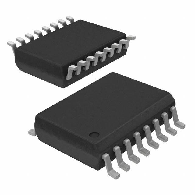
The MIC5891 is available in a 16-pin plastic DIP
package (N) and 16-pin wide SOIC package (WM).
OUT5
DS20005638A-page 1
�MIC5891
Functional Diagram
MIC5891
16-PIN PDIP OR SOICW
CLOCK
SERIAL
DATA IN
8-BIT SERIAL PARALLEL SHIFT REGISTER
STROBE
LATCHES
SERIAL
DATA OUT
OUTPUT
ENABLE
GROUND
MOS
BIPOLAR
OUT1 OUT2
DS20005638A-page 2
OUT3 OUT4 OUT5
OUT6 OUT7 OUT8
2016 Microchip Technology Inc.
�MIC5891
1.0
ELECTRICAL CHARACTERISTICS
Absolute Maximum Ratings † (Note 1, Note 2, Note 3)
Output Voltage (VOUT) ..............................................................................................................................................+50V
Logic Supply Voltage Range (VDD) ............................................................................................................ +4.5V to +15V
Load Supply Voltage Range (VBB) ............................................................................................................. +5.0V to +50V
Input Voltage Range (VIN) .............................................................................................................. –0.3V to (VDD + 0.3V)
Continuous Collector Current (IC) .........................................................................................................................500 mA
Package Power Dissipation ...................................................................................................................... See Figure 2-1
† Notice: Stresses above those listed under “Absolute Maximum Ratings” may cause permanent damage to the device.
This is a stress rating only and functional operation of the device at those or any other conditions above those indicated
in the operational sections of this specification is not intended. Exposure to maximum rating conditions for extended
periods may affect device reliability.
Note 1: TA = +25°C.
2: Derate at the rate of 20 mW/°C above TA = +25°C.
3: Microchip CMOS devices have input-static protection, but are susceptible to damage when exposed to
extremely high static electrical charges.
TABLE 1-1:
ALLOWABLE DUTY CYCLES
Maximum Allowable Duty Cycles at a TA of:
Number of Outputs ON at
IOUT = –200 mA
+50°C
+60°C
+70°C
8
53%
47%
41%
7
60%
54%
48%
6
70%
64%
56%
5
83%
75%
67%
4
100%
94%
84%
3
100%
100%
100%
2
100%
100%
100%
1
100%
100%
100%
2016 Microchip Technology Inc.
DS20005638A-page 3
�MIC5891
TABLE 1-2:
ELECTRICAL CHARACTERISTICS
Electrical Characteristics: VBB = 50V, VDD = 5V to 12V; TA = 25°C, unless noted. (Note 1).
Parameters
Output Leakage Current
Output Saturation Voltage
Output Sustaining Voltage
Input Voltage
Input Current
Input Impedance
Maximum Clock Frequency
Sym.
ICEX
VCE(SAT)
VCE(SUS)
VIN(1)
VIN(0)
IIN(1)
ZIN
fc
Min.
Typ.
Max.
Units
Conditions
—
—
–50
µA
TA = +25°C
—
—
–100
µA
TA = +85°C
—
—
2.3
V
IOUT = –100 mA, TA = +85°C
—
—
2.4
V
IOUT = –225 mA, TA = +85°C
—
—
2.5
V
IOUT = –350 mA, TA = +85°C
35
—
—
V
IOUT = –350 mA, L = 2 mH
3.5
—
VDD+0.3
V
VDD = 5.0V
10.5
—
VDD+0.3
V
VDD = 12V
VSS–0.3
—
0.8
V
VDD = 5.0V to 12V
—
—
120
µA
VDD = VIN = 5.0V
—
—
240
µA
VDD = 12V
100
—
—
kΩ
VDD = 5.0V
50
—
—
kΩ
VDD = 12V
3.3
—
—
MHz
—
—
—
20
kΩ
VDD = 5.0V
—
—
6.0
kΩ
VDD = 12V
Serial Data Output Resistance
ROUT
Turn-On Delay
tPLH
—
—
2.0
µs
Output Enable to Output,
IOUT = –350 mA
Turn-Off Delay
tPHL
—
—
10
µs
Output Enable to Output,
IOUT = –350 mA
—
—
10
mA
All outputs on, all outputs open
—
—
200
µA
All outputs off
—
—
100
µA
VDD = 5V, all outputs off,
inputs = 0V
—
—
200
µA
VDD = 12V, all outputs off,
inputs = 0V
—
—
1.0
mA
VDD = 5V, one output on,
inputs = 0V
—
—
3.0
mA
VDD = 12V, one output on,
inputs = 0V
—
—
50
µA
TA = +25°C; Max. VBB
—
—
100
µA
TA = +85°C; Max. VBB
—
—
2.0
V
IF = 350 mA; VBB open
IBB
Supply Current
IDD
Diode Leakage Current
IH
Diode Forward Voltage
VF
Note 1:
2:
3:
Specification for packaged product only.
Positive (negative) current is defined as going into (coming out of) the specified device pin.
Operation of these devices with standard TTL may require the use of appropriate pull-up resistors.
DS20005638A-page 4
2016 Microchip Technology Inc.
�MIC5891
TEMPERATURE SPECIFICATIONS
Parameters
Sym.
Min.
Typ.
Max.
Units
Conditions
Operating Temperature Range
TA
–40
—
+85
°C
Note 1
Storage Temperature Range
TS
–65
—
+150
°C
—
Temperature Ranges
Note 1:
The maximum allowable power dissipation is a function of ambient temperature, the maximum allowable
junction temperature and the thermal resistance from junction to air (i.e., TA, TJ, JA). Exceeding the
maximum allowable power dissipation will cause the device operating junction temperature to exceed the
maximum +125°C rating. Sustained junction temperatures above +125°C can impact the device reliability.
Typical Circuits
V BB
V DD
IN
V OUT
FIGURE 1-1:
Typical Input Circuit
2016 Microchip Technology Inc.
FIGURE 1-2:
Typical Output Circuit.
DS20005638A-page 5
�MIC5891
2.0
The graphs and tables provided following this note are a statistical summary based on a limited number of
samples and are provided for informational purposes only. The performance characteristics listed herein
are not tested or guaranteed. In some graphs or tables, the data presented may be outside the specified
operating range (e.g., outside specified power supply range) and therefore outside the warranted range.
PACKAGE POWER DISSIPATION (W)
Note:
TYPICAL PERFORMANCE CURVES
2.5
2
PDIP
șJA = 60°C/W
1.5
1
0.5
CerDIP
șJA = 90°C/W
0
25
50
75
100 125 150
AMBIENT TEMPERATURE (°C)
FIGURE 2-1:
Allowable Package Power
Dissipation vs. Temperature.
DS20005638A-page 6
2016 Microchip Technology Inc.
�MIC5891
3.0
TIMING CONDITIONS
The descriptions of the timing conditions are listed below Figure 3-1.
CLOCK
A
B
D
DATA IN
E
F
C
STROBE
OUTPUT
ENABLE
G
OUT N
H
FIGURE 3-1:
TABLE 3-1:
I
Timing Conditions.
TIMING CONDITIONS PARAMETERS
VDD = 5.0V, Logic levels are VDD and ground.
Reference
A
Parameter
Value
Minimum data active time before clock pulse (data set-up time)
75 ns
B
Minimum data active time after clock pulse (data hold time)
75 ns
C
Minimum data pulse width
150 ns
D
Minimum clock pulse width
150 ns
E
Minimum time between clock activation and strobe
300 ns
F
Minimum strobe pulse width
100 ns
G
Typical time between strobe activation and output transition
1.0 µs
H
Turn-off delay
See Electrical Characteristics
I
Turn-on delay
See Electrical Characteristics
TABLE 3-2:
Serial
Data
Input
TRUTH TABLE
Clock
Input
Shift Register
Contents
I1 I2 I3 ... IN-1 IN
Serial
Data
Output
H
H R1 R2 ... RN-2 RN-1
RN-1
L
L R1 R2 ... RN-2 RN-1
RN-1
X
R1 R2 R3 ... RN-1 RN
RN
X X X ... X X
P1 P2 P3 ... PN-1 PN
—
—
Strobe
Input
Latch Contents
Output Content
Output
Enable
I1 I2 I3 ... IN-1 IN
—
—
X
L
R1 R2 R3 ... RN-1 RN
PN
H
P1 P2 P3 ... PN-1 PN
I1 I2 I3 ... IN-1 IN
—
—
L
P1 P2 P3 ... PN-1 PN
—
—
—
X X X ... X X
H
L = Low Logic Level, H = High Logic Level, X = Irrelevant, P = Present State, R = Previous State.
2016 Microchip Technology Inc.
L L L ... L L
DS20005638A-page 7
�MIC5891
4.0
APPLICATION INFORMATION
Serial data present at the input is transferred into the
shift register on the rising edge of the CLOCK input
pulse. Additional CLOCK pulses shift data information
towards the SERIAL DATA OUTPUT. The serial data
must appear at the input prior to the rising edge of the
CLOCK input waveform.
The 8 bits present in the shift register are transferred to
the respective latches when the STROBE is high
(serial-to-parallel conversion). The latches will continue
to accept new data as long as the STROBE is held
high. Most applications where the latching feature is
not used (STROBE tied high) require the OUTPUT
ENABLE input to be high during serial data entry.
Outputs are active (controlled by the latch state) when
the OUTPUT ENABLE is low. All outputs are low
(disabled) when the OUTPUT ENABLE is high.
OUTPUT ENABLE does not affect the data in the shift
register or latch.
DS20005638A-page 8
2016 Microchip Technology Inc.
�MIC5891
5.0
PACKAGING INFORMATION
5.1
Package Marking Information
16-Pin PDIP*
XXXXXX
XXXXXXXXX
YYWW
16-Pin SOICW*
XXXXXX
XXXXXXXXXX
YYWW
Legend: XX...X
Y
YY
WW
NNN
e3
*
Example
MICREL
MIC5891YN
1312
Example
MICREL
MIC5891YWM
1632
Product code or customer-specific information
Year code (last digit of calendar year)
Year code (last 2 digits of calendar year)
Week code (week of January 1 is week ‘01’)
Alphanumeric traceability code
Pb-free JEDEC® designator for Matte Tin (Sn)
This package is Pb-free. The Pb-free JEDEC designator ( e3 )
can be found on the outer packaging for this package.
●, ▲, ▼ Pin one index is identified by a dot, delta up, or delta down (triangle
mark).
Note:
In the event the full Microchip part number cannot be marked on one line, it will
be carried over to the next line, thus limiting the number of available
characters for customer-specific information. Package may or may not include
the corporate logo.
Underbar (_) and/or Overbar (⎯) symbol may not be to scale.
2016 Microchip Technology Inc.
DS20005638A-page 9
�MIC5891
16-Lead PDIP Package Outline and Recommended Land Pattern
Note:
For the most current package drawings, please see the Microchip Packaging Specification located at
http://www.microchip.com/packaging.
DS20005638A-page 10
2016 Microchip Technology Inc.
�MIC5891
16-Lead SOICW Package Outline and Recommended Land Pattern
Note:
For the most current package drawings, please see the Microchip Packaging Specification located at
http://www.microchip.com/packaging.
2016 Microchip Technology Inc.
DS20005638A-page 11
�MIC5891
NOTES:
DS20005638A-page 12
2016 Microchip Technology Inc.
�MIC5891
APPENDIX A:
REVISION HISTORY
Revision A (October 2016)
• Converted Micrel document MIC5891 to Microchip data sheet DS20005638A.
• Minor text changes throughout.
• Operating temperature range corrected in the
Temperature Specifications section.
• Maximum Saturation Voltage values updated in
Table 1-2.
• First Input Current maximum value updated in
Table 1-2.
2016 Microchip Technology Inc.
DS20005638A-page 13
�MIC5891
NOTES:
DS20005638A-page 14
2016 Microchip Technology Inc.
�MIC5891
PRODUCT IDENTIFICATION SYSTEM
To order or obtain information, e.g., on pricing or delivery, contact your local Microchip representative or sales office.
PART NO.
XX
X
–
Examples:
X.X
a) MIC5891YN:
8-Bit Serial-Input Latched
Source Driver, –40°C to +85°C
Junction Temperature Range,
16-Lead PDIP, 25/Tube
a) MIC5891YWM:
8-Bit Serial-Input Latched
Source Driver, –40°C to +85°C
Junction Temperature Range,
16-Lead SOICW, 47/Tube
a) MIC5891YWM-TR:
8-Bit Serial-Input Latched
Source Driver, –40°C to +85°C
Junction Temperature Range,
16-Lead SOICW, 1,000/Reel
Device
Junction Package Media Type
Temperature Range
Device:
MIC5891:
Junction
Temperature
Range:
Y
Package:
N
=
WM =
Media Type:
TR
= 1,000/Reel for WM Package
(blank)= 25/Tube for N Package
(blank)= 47/Tube for WM Package
=
8-Bit Serial-Input Latched Source Driver
–40°C to +85°C
16-Lead PDIP
16-Lead SOICW
2016 Microchip Technology Inc.
DS20005638A-page 15
�MIC5891
NOTES:
DS20005638A-page 16
2016 Microchip Technology Inc.
�Note the following details of the code protection feature on Microchip devices:
•
Microchip products meet the specification contained in their particular Microchip Data Sheet.
•
Microchip believes that its family of products is one of the most secure families of its kind on the market today, when used in the
intended manner and under normal conditions.
•
There are dishonest and possibly illegal methods used to breach the code protection feature. All of these methods, to our
knowledge, require using the Microchip products in a manner outside the operating specifications contained in Microchip’s Data
Sheets. Most likely, the person doing so is engaged in theft of intellectual property.
•
Microchip is willing to work with the customer who is concerned about the integrity of their code.
•
Neither Microchip nor any other semiconductor manufacturer can guarantee the security of their code. Code protection does not
mean that we are guaranteeing the product as “unbreakable.”
Code protection is constantly evolving. We at Microchip are committed to continuously improving the code protection features of our
products. Attempts to break Microchip’s code protection feature may be a violation of the Digital Millennium Copyright Act. If such acts
allow unauthorized access to your software or other copyrighted work, you may have a right to sue for relief under that Act.
Information contained in this publication regarding device
applications and the like is provided only for your convenience
and may be superseded by updates. It is your responsibility to
ensure that your application meets with your specifications.
MICROCHIP MAKES NO REPRESENTATIONS OR
WARRANTIES OF ANY KIND WHETHER EXPRESS OR
IMPLIED, WRITTEN OR ORAL, STATUTORY OR
OTHERWISE, RELATED TO THE INFORMATION,
INCLUDING BUT NOT LIMITED TO ITS CONDITION,
QUALITY, PERFORMANCE, MERCHANTABILITY OR
FITNESS FOR PURPOSE. Microchip disclaims all liability
arising from this information and its use. Use of Microchip
devices in life support and/or safety applications is entirely at
the buyer’s risk, and the buyer agrees to defend, indemnify and
hold harmless Microchip from any and all damages, claims,
suits, or expenses resulting from such use. No licenses are
conveyed, implicitly or otherwise, under any Microchip
intellectual property rights unless otherwise stated.
Trademarks
The Microchip name and logo, the Microchip logo, AnyRate,
dsPIC, FlashFlex, flexPWR, Heldo, JukeBlox, KeeLoq,
KeeLoq logo, Kleer, LANCheck, LINK MD, MediaLB, MOST,
MOST logo, MPLAB, OptoLyzer, PIC, PICSTART, PIC32 logo,
RightTouch, SpyNIC, SST, SST Logo, SuperFlash and UNI/O
are registered trademarks of Microchip Technology
Incorporated in the U.S.A. and other countries.
ClockWorks, The Embedded Control Solutions Company,
ETHERSYNCH, Hyper Speed Control, HyperLight Load,
IntelliMOS, mTouch, Precision Edge, and QUIET-WIRE are
registered trademarks of Microchip Technology Incorporated
in the U.S.A.
Analog-for-the-Digital Age, Any Capacitor, AnyIn, AnyOut,
BodyCom, chipKIT, chipKIT logo, CodeGuard, dsPICDEM,
dsPICDEM.net, Dynamic Average Matching, DAM, ECAN,
EtherGREEN, In-Circuit Serial Programming, ICSP, Inter-Chip
Connectivity, JitterBlocker, KleerNet, KleerNet logo, MiWi,
motorBench, MPASM, MPF, MPLAB Certified logo, MPLIB,
MPLINK, MultiTRAK, NetDetach, Omniscient Code
Generation, PICDEM, PICDEM.net, PICkit, PICtail,
PureSilicon, RightTouch logo, REAL ICE, Ripple Blocker,
Serial Quad I/O, SQI, SuperSwitcher, SuperSwitcher II, Total
Endurance, TSHARC, USBCheck, VariSense, ViewSpan,
WiperLock, Wireless DNA, and ZENA are trademarks of
Microchip Technology Incorporated in the U.S.A. and other
countries.
SQTP is a service mark of Microchip Technology Incorporated
in the U.S.A.
Microchip received ISO/TS-16949:2009 certification for its worldwide
headquarters, design and wafer fabrication facilities in Chandler and
Tempe, Arizona; Gresham, Oregon and design centers in California
and India. The Company’s quality system processes and procedures
are for its PIC® MCUs and dsPIC® DSCs, KEELOQ® code hopping
devices, Serial EEPROMs, microperipherals, nonvolatile memory and
analog products. In addition, Microchip’s quality system for the design
and manufacture of development systems is ISO 9001:2000 certified.
QUALITY MANAGEMENT SYSTEM
CERTIFIED BY DNV
== ISO/TS 16949 ==
2016 Microchip Technology Inc.
Silicon Storage Technology is a registered trademark of
Microchip Technology Inc. in other countries.
GestIC is a registered trademarks of Microchip Technology
Germany II GmbH & Co. KG, a subsidiary of Microchip
Technology Inc., in other countries.
All other trademarks mentioned herein are property of their
respective companies.
© 2016, Microchip Technology Incorporated, Printed in the
U.S.A., All Rights Reserved.
ISBN: 978-1-5224-1034-8
DS20005638A-page 17
�Worldwide Sales and Service
AMERICAS
ASIA/PACIFIC
ASIA/PACIFIC
EUROPE
Corporate Office
2355 West Chandler Blvd.
Chandler, AZ 85224-6199
Tel: 480-792-7200
Fax: 480-792-7277
Technical Support:
http://www.microchip.com/
support
Web Address:
www.microchip.com
Asia Pacific Office
Suites 3707-14, 37th Floor
Tower 6, The Gateway
Harbour City, Kowloon
China - Xiamen
Tel: 86-592-2388138
Fax: 86-592-2388130
Austria - Wels
Tel: 43-7242-2244-39
Fax: 43-7242-2244-393
China - Zhuhai
Tel: 86-756-3210040
Fax: 86-756-3210049
Denmark - Copenhagen
Tel: 45-4450-2828
Fax: 45-4485-2829
India - Bangalore
Tel: 91-80-3090-4444
Fax: 91-80-3090-4123
France - Paris
Tel: 33-1-69-53-63-20
Fax: 33-1-69-30-90-79
India - New Delhi
Tel: 91-11-4160-8631
Fax: 91-11-4160-8632
Germany - Dusseldorf
Tel: 49-2129-3766400
Atlanta
Duluth, GA
Tel: 678-957-9614
Fax: 678-957-1455
Hong Kong
Tel: 852-2943-5100
Fax: 852-2401-3431
Australia - Sydney
Tel: 61-2-9868-6733
Fax: 61-2-9868-6755
China - Beijing
Tel: 86-10-8569-7000
Fax: 86-10-8528-2104
Austin, TX
Tel: 512-257-3370
China - Chengdu
Tel: 86-28-8665-5511
Fax: 86-28-8665-7889
Boston
Westborough, MA
Tel: 774-760-0087
Fax: 774-760-0088
China - Chongqing
Tel: 86-23-8980-9588
Fax: 86-23-8980-9500
Chicago
Itasca, IL
Tel: 630-285-0071
Fax: 630-285-0075
Cleveland
Independence, OH
Tel: 216-447-0464
Fax: 216-447-0643
Dallas
Addison, TX
Tel: 972-818-7423
Fax: 972-818-2924
Detroit
Novi, MI
Tel: 248-848-4000
Houston, TX
Tel: 281-894-5983
Indianapolis
Noblesville, IN
Tel: 317-773-8323
Fax: 317-773-5453
Los Angeles
Mission Viejo, CA
Tel: 949-462-9523
Fax: 949-462-9608
New York, NY
Tel: 631-435-6000
San Jose, CA
Tel: 408-735-9110
Canada - Toronto
Tel: 905-695-1980
Fax: 905-695-2078
China - Dongguan
Tel: 86-769-8702-9880
China - Guangzhou
Tel: 86-20-8755-8029
China - Hangzhou
Tel: 86-571-8792-8115
Fax: 86-571-8792-8116
China - Hong Kong SAR
Tel: 852-2943-5100
Fax: 852-2401-3431
China - Nanjing
Tel: 86-25-8473-2460
Fax: 86-25-8473-2470
China - Qingdao
Tel: 86-532-8502-7355
Fax: 86-532-8502-7205
China - Shanghai
Tel: 86-21-5407-5533
Fax: 86-21-5407-5066
China - Shenyang
Tel: 86-24-2334-2829
Fax: 86-24-2334-2393
China - Shenzhen
Tel: 86-755-8864-2200
Fax: 86-755-8203-1760
India - Pune
Tel: 91-20-3019-1500
Japan - Osaka
Tel: 81-6-6152-7160
Fax: 81-6-6152-9310
Japan - Tokyo
Tel: 81-3-6880- 3770
Fax: 81-3-6880-3771
Korea - Daegu
Tel: 82-53-744-4301
Fax: 82-53-744-4302
Korea - Seoul
Tel: 82-2-554-7200
Fax: 82-2-558-5932 or
82-2-558-5934
Malaysia - Kuala Lumpur
Tel: 60-3-6201-9857
Fax: 60-3-6201-9859
Malaysia - Penang
Tel: 60-4-227-8870
Fax: 60-4-227-4068
Philippines - Manila
Tel: 63-2-634-9065
Fax: 63-2-634-9069
Germany - Karlsruhe
Tel: 49-721-625370
Germany - Munich
Tel: 49-89-627-144-0
Fax: 49-89-627-144-44
Italy - Milan
Tel: 39-0331-742611
Fax: 39-0331-466781
Italy - Venice
Tel: 39-049-7625286
Netherlands - Drunen
Tel: 31-416-690399
Fax: 31-416-690340
Poland - Warsaw
Tel: 48-22-3325737
Spain - Madrid
Tel: 34-91-708-08-90
Fax: 34-91-708-08-91
Sweden - Stockholm
Tel: 46-8-5090-4654
UK - Wokingham
Tel: 44-118-921-5800
Fax: 44-118-921-5820
Singapore
Tel: 65-6334-8870
Fax: 65-6334-8850
Taiwan - Hsin Chu
Tel: 886-3-5778-366
Fax: 886-3-5770-955
Taiwan - Kaohsiung
Tel: 886-7-213-7828
China - Wuhan
Tel: 86-27-5980-5300
Fax: 86-27-5980-5118
Taiwan - Taipei
Tel: 886-2-2508-8600
Fax: 886-2-2508-0102
China - Xian
Tel: 86-29-8833-7252
Fax: 86-29-8833-7256
Thailand - Bangkok
Tel: 66-2-694-1351
Fax: 66-2-694-1350
06/23/16
DS20005638A-page 18
2016 Microchip Technology Inc.
�